
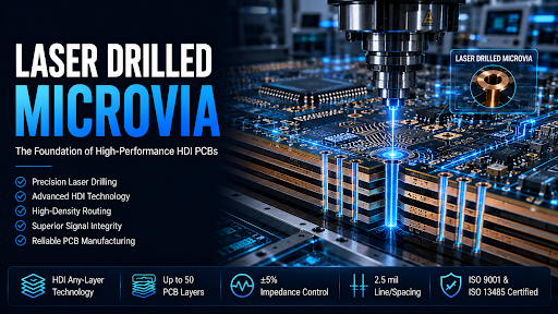
As electronic devices continue to become smaller, faster, and more powerful, printed circuit boards must support more components in less space. Industries such as telecommunications, medical technology, aerospace, automotive electronics, and consumer devices all depend on advanced PCB designs to achieve high performance. Laser drilled microvia technology enables these high-density interconnections and is widely used in High-Density Interconnect (HDI) PCBs to achieve precise, compact, and reliable designs.
Microvias allow engineers to build compact multilayer circuit boards with excellent signal performance and improved routing flexibility. However, manufacturing HDI boards with laser-drilled microvias requires advanced equipment, precise fabrication, and strict quality control. Choosing an experienced hdi pcb manufacturer is essential for producing reliable HDI PCBs that meet today’s demanding electrical and mechanical performance requirements.
What Is a Laser Drilled Microvia?
A laser-drilled microvia is a very small hole created with laser technology to connect adjacent layers of an HDI printed circuit board. Unlike traditional mechanically drilled vias, laser-drilled microvias typically have much smaller diameters and shallower depths, allowing designers to increase routing density while reducing signal path length.
Typical microvias are designed with controlled microvia diameter and depth, and manufacturers must carefully manage the microvia aspect ratio (depth-to-diameter ratio) to achieve reliable copper plating. Proper capture pad and target pad design is also essential to ensure accurate laser registration and dependable electrical connections.
Microvias are commonly used in:
- Smartphones
- Medical devices
- 5G communication equipment
- Industrial control systems
- Aerospace electronics
- Automotive electronics
- Wearable technology
These applications require compact circuit boards that deliver reliable electrical performance in limited space.
Why Microvias Are Important in HDI PCBs
Modern electronic products continue to shrink while offering more functionality. Traditional PCB designs often cannot support the routing density needed for today’s advanced components.
Laser-drilled microvias solve this challenge by providing several important advantages.
Higher Circuit Density
Smaller vias create more routing space, allowing engineers to place additional components and routing channels within a compact PCB footprint.
Better Signal Integrity
Shorter electrical paths reduce parasitic inductance and capacitance, helping maintain signal quality in high-speed and high-frequency applications.
Improved Electrical Performance
Because microvias connect only the required layers, they reduce unnecessary stub effects and improve overall electrical performance.
Smaller Product Size
Higher routing density allows designers to reduce PCB dimensions, enabling thinner, lighter, and more compact electronic products.
These advantages make laser-drilled microvias a key enabling technology for modern HDI circuit boards.
Advanced HDI Design Considerations
Not all microvia structures are the same. Depending on routing complexity, designers may use stacked microvias or staggered microvias.
- Stacked microvias are positioned directly on top of one another and often require copper filling before additional layers are laminated.
- Staggered microvias are offset between layers, reducing mechanical stress while simplifying fabrication in many designs.
Many HDI designs also use via-in-pad technology to maximize routing space beneath fine-pitch components. These vias are typically copper filled and planarized before surface finishing to provide a flat soldering surface.
Complex HDI constructions often require sequential lamination, where additional dielectric and copper layers are laminated in multiple manufacturing cycles. This process enables higher interconnect density while maintaining precise layer registration.
Why Manufacturing Precision Matters
Although microvias offer significant advantages, they also require exceptional manufacturing accuracy.
Successful HDI fabrication depends on:
- Precise laser drilling
- Accurate layer registration
- Controlled microvia diameter and depth
- Uniform copper filling and plating
- Reliable impedance control
- Clean via walls
Even small process variations can create defects that reduce long-term reliability.
Potential manufacturing issues include:
- Plating voids inside microvias
- Corner cracks caused by thermal stress
- Interface separation between copper and dielectric materials
- Poor copper filling in stacked microvias
These defects can eventually lead to intermittent electrical failures, particularly in products exposed to repeated thermal cycling.
Advanced HDI Manufacturing Capabilities
As an experienced HDI PCB manufacturer, Fast Turn PCB supports demanding HDI applications with capabilities including:
- HDI 1+N+1 through Any-Layer construction with 10-day delivery
- High-layer-count PCB fabrication up to 50 layers
- Minimum line width and spacing of 2.5 mils
- Impedance control tolerance as tight as ±5%
These capabilities support compact, high-density PCB designs used in communications, medical, aerospace, and industrial applications.
Tight Impedance Control for High-Speed Designs
Many HDI boards operate in high-speed communication systems where signal integrity is critical.
Fast Turn PCB maintains impedance control tolerance as tight as ±5%, helping ensure reliable signal transmission for applications including:
- 5G infrastructure
- Networking equipment
- High-speed computing
- Medical imaging systems
- Aerospace electronics
Accurate impedance control reduces signal reflections and helps maintain consistent electrical performance throughout complex multilayer boards.
Quality Control for Reliable Microvias
Reliable HDI manufacturing requires more than precision drilling. Comprehensive inspection and testing help verify that every microvia performs as intended.
Fast Turn PCB applies multiple quality-control methods, including:
- Automated Optical Inspection (AOI)
- Electrical testing
- Microsection analysis
- Thermal cycling validation where required
Microsection analysis allows engineers to examine plated microvias, verify copper thickness, detect plating voids, evaluate interface integrity, and confirm complete copper filling. Thermal cycling further evaluates long-term reliability by exposing the PCB to repeated temperature changes that simulate real operating conditions.
Certified Manufacturing Standards
Reliable HDI PCB manufacturing depends on strict quality management throughout every stage of production.
Fast Turn PCB follows internationally recognized standards, including:
- ISO9001 certification
- ISO13485 certification
- IPC Class 3 compliance
These certifications demonstrate the company’s commitment to producing dependable PCBs for industries where precision and reliability are essential.
Why Engineers Choose Fast Turn PCB
Developing HDI PCBs requires more than advanced equipment. Engineers need a manufacturing partner with experience in laser-drilled microvias, sequential lamination, controlled impedance, and complex multilayer fabrication.
Fast Turn PCB combines advanced manufacturing technology, experienced engineering teams, precision fabrication, and comprehensive quality control to support projects from prototype development through high-volume production.
Whether designing communication equipment, medical devices, industrial automation systems, automotive electronics, or aerospace technology, customers benefit from dependable manufacturing, responsive technical support, and consistent production quality.
Conclusion
Laser-drilled microvias have become an essential part of modern HDI PCB technology, enabling higher circuit density, improved signal integrity, and smaller product sizes for advanced electronic devices.
Working with an experienced hdi pcb manufacturer helps ensure every HDI PCB is manufactured with the precision, process control, and quality verification required for demanding applications. Fast Turn PCB combines advanced HDI manufacturing capabilities, tight impedance control, sequential lamination expertise, and rigorous quality inspection to support the next generation of high-performance electronic products.
Visit fastturnpcbs.com today to explore professional HDI PCB manufacturing solutions and discover how its advanced capabilities can support your next high-performance electronics project.












Leave a Reply